
One.MIT Creates a Monument—at the Smallest Scale
-
-
Slice of MIT
- 4
Filed Under


MIT.nano is a natural convening space. The Institute’s newest laboratory facility, devoted to nanoscale research, sits in the very center of campus as an open toolset available to researchers from across MIT and beyond. Its public spaces are frequently crowded with students huddling over problem sets and steady flows of visitors peeking through the building’s glass walls and windows to get a glimpse of the wonders of modern science and technology in action.
When the building opened last fall, its inaugural faculty director, Vladimir Bulović, decided to take this convening power a step further. “MIT.nano sits in the shadow of MIT’s Great Dome, and our responsibility is to enhance the work and aspirations of the entire campus,” says Bulović, the Fariborz Maseeh (1990) Professor in Emerging Technology. “We wanted a way to celebrate all of us instead of just a few — a monument to the MIT community made using the tools of nanoscale research.”
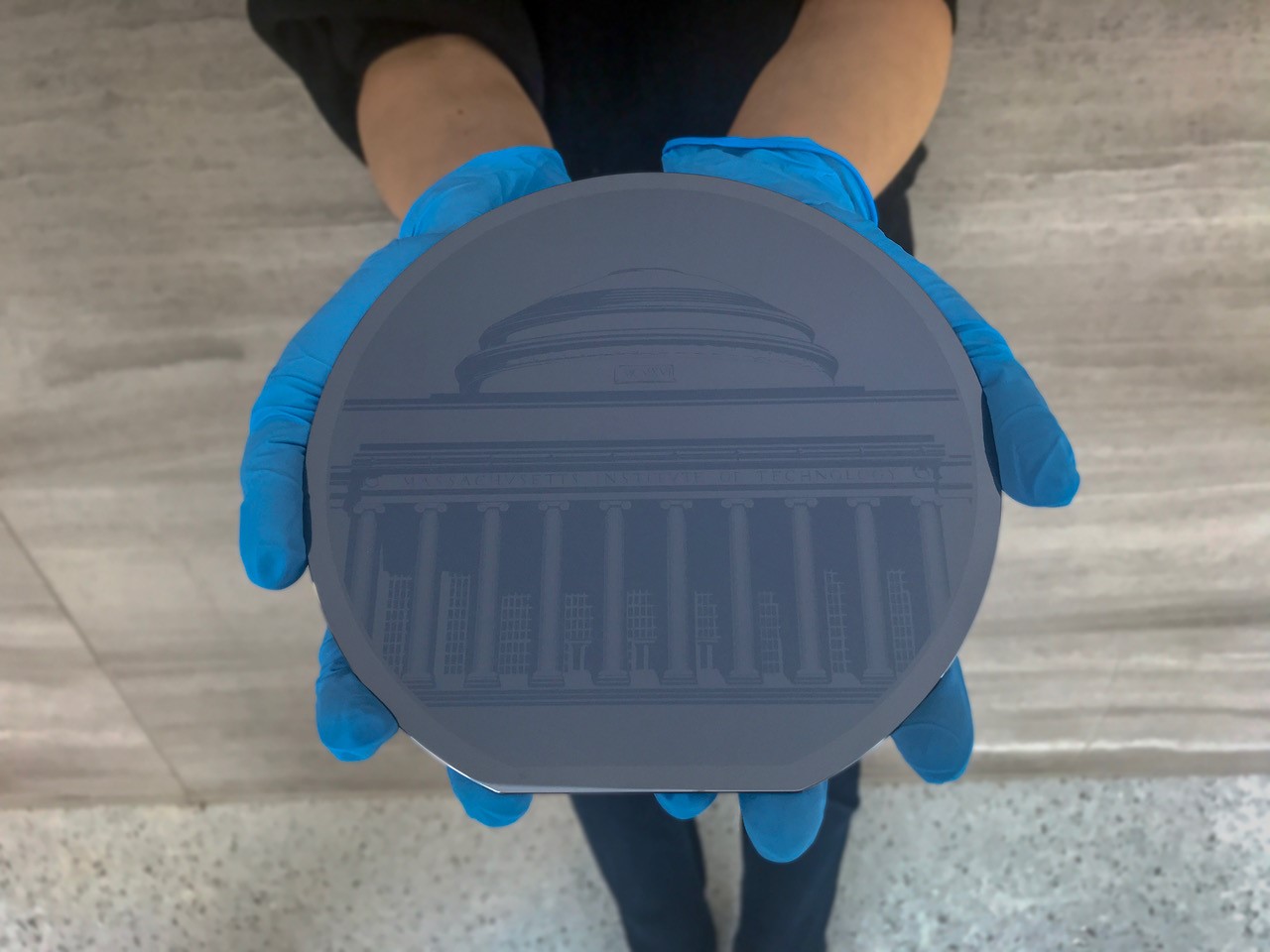
The result is “One.MIT,” a mosaic depicting the MIT Great Dome formed by etching more than 270,000 names on a 6-inch-diameter silicon wafer. The image attempts to include the names of all the individuals associated with MIT between its founding in 1861 and Spring 2018 — every student, alumnus/a, professor, president, lecturer, lab assistant, staff member, custodian, administrator, and anyone else who has been a member of the MIT community.
Now on display in the MIT.nano first-floor gallery, the “One.MIT” wafer hangs alongside a 6-foot diameter enlargement as a permanent installation celebrating the many generations of MIT that are the foundation and inspiration for the research that will take place inside MIT.nano. Because the names are too small to see with the naked eye, a new website, onemit.mit.edu, enables anyone to search for a name and find its location in the mosaic.
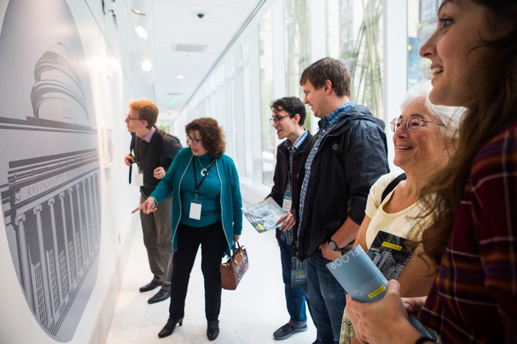
Members of the MIT community view the six-foot diameter enlargement hanging in the MIT.nano building.
“A bit of a goose chase”
Collecting the names that would make up “One.MIT” was the first challenge. Annie Wang, a research scientist and special projects coordinator for MIT.nano, embraced solving this puzzle. The initial stage, she says, was pretty easy: the MIT Alumni Association has a comprehensive database of all degree recipients and former students, and the Office of Institutional Research could provide records of faculty and staff — but only back to 1991.
“Everything before then,” Wang says, “was a bit of a goose chase.” Joining Wang on the chase were staff from the MIT Libraries and Institute Archives, and W. Craig Carter, the POSCO Professor of Materials Science and Engineering, who also happens to do computational art projects in his spare time.
Working with scans of more than 6,000 pages of MIT’s old paper directories, Carter, Wang, and two volunteers built specialized algorithms and machine learning tools to extract the remaining data for the project. “Some things gave us no end of trouble,” Carter says. “Like ‘Doc’ Edgerton’s name always appearing in parentheses.”
Then things got even more difficult, Wang says: “It turns out that what’s really hard is to arrange all of the names into the picture.” Once again, Carter found his programming skills taxed in new ways. To have the names draw a shape, each of their roughly 4 million typographic characters had to be converted to a format in which Carter could adjust their shading — to “draw” the image — and manage their spacing to maximally fill the available space in an aesthetically sophisticated way that resulted in an image of the MIT dome.
Etching a monument at the micro- and nanoscale
The output of Carter and Wang’s initial efforts, however beautiful, was only the first step for what they needed. “One.MIT” also needed to exist as a set of detailed computer-aided design (CAD) drawings and instructions that could be used in micro- and nanotechnology fabrication processes. Carter says he was intrigued by the opportunity to learn how to convert his PDF document into a set of CAD drawings, but, he deadpans: “I have a rule about these things. If you make a prediction about how long something new is going to take you, you should multiply your estimate twice, then go to the next unit. So, two days? That’s eight weeks.”
He passed his files to Wang, who worked with technical staff in the Microsystems Technology Laboratories (MTL) to set about creating a silicon wafer etched with the same information. But the MTL’s equipment and processes — including oxidation furnaces, photolithography tools, and photoresist coaters — are more suited to the highly repetitive patterns of manufacturing priorities than they are to names, alphabets, and the aesthetic considerations of artwork. “Normally, MTL works with CAD files that are a few hundred kilobytes,” says Wang. “They told me the largest they’d ever worked with before us was about one gig. Ours was about 4 gigabytes.”
By placing One.MIT in our most visible corner, we’re reminding everyone that the people of MIT are our most incredible resource—just as they have been since the beginning.
A wafer was completed in time to be installed on the first-floor gallery of MIT.nano for the facility’s grand opening on Oct. 4, 2018. The final element of “One.MIT” is the website, just launched this week, in which users can find and locate any of the names in the project. The organizers, who spent weeks reviewing the names on the lists, are confident the project represents a solid and comprehensive accounting of the MIT community. “I wouldn’t call it perfect,” Wang explains, “but we really did our best.”
For Bulović, “One.MIT” is the first step in what he sees as a key objective for MIT.nano: to be a place where all kinds of people can make unforeseen connections and pursue their ideas with creativity, intelligence, and passion. “It would be understandable to see MIT.nano as just a collection of tools and instruments,” he says. “By placing 'One.MIT' in our most visible corner, we’re reminding everyone that the people of MIT are our most incredible resource — just as they have been since the beginning.”
For best results, usage of a desktop browser (rather than a mobile device) is recommended to access onemit.mit.edu. Are you a degreed or non-degreed MIT alumnus/a and can't find your name? Please email the MIT Alumni Association at mitalum@mit.edu and provide your full name, date of birth, dates of attendance, and course/degree information so that we may verify your status. You may also wish to review the alumni/ae membership criteria.


Comments
Judith Yanowitz
Mon, 03/18/2019 9:49pm
onemit
I applaud the inclusion of all MIT-affiliates on the onemit nanodisk. However, I curious about the decision to list people with their married names rather the ones they used while at MIT. Fortunately, this is inclusive for women and men who changed their names. It just makes it a challenge to connect names to the person while they were actually at MIT (although once a student; always an alum).
Alfonso Govela
Tue, 03/19/2019 12:00pm
(No subject)
Great idea! Congrats! Can I get one?
Nicole Taylor
Wed, 03/20/2019 4:01pm
(No subject)
Currently there aren’t any replicas or prints available, but it’s great to know of your interest in that. Thanks!
Tom Forest
Tue, 03/19/2019 3:09pm
questions on specs
What's the silicon feature size? What's the font and its size? Where was it fabricated?